Photovoltaics and Optoelectronics from 2D Semiconductors
Two-dimensional (2-D) materials research done in the Escarra lab is a multidisciplinary effort to create large scale technologies from atomically flat materials. Since the renewed interest in the properties of graphene in 2004, 2-D materials have experienced a boom in research and development that has led to the discovery of a many new 2-D materials and characteristics. These two dimensional materials are stable, flexible, strong, and possess a wealth of qualities that could enable electronics to be made smaller and better than previously thought possible. For example, graphene can conduct electrons with great efficiency and has unparalleled strength. Monolayer molybdenum disulfide is a 2-dimensionsal direct-bandgap semiconductor that can be used to fabricate photodetectors, light emitters, and solar cells. These materials have already shown great promise, and many more remain to be discovered; the race is on to synthesize these materials with high quality and large quantity.
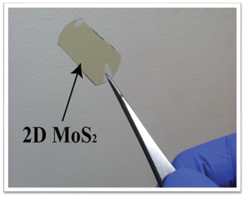
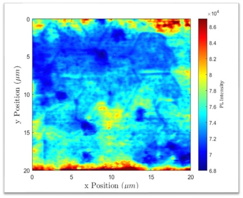
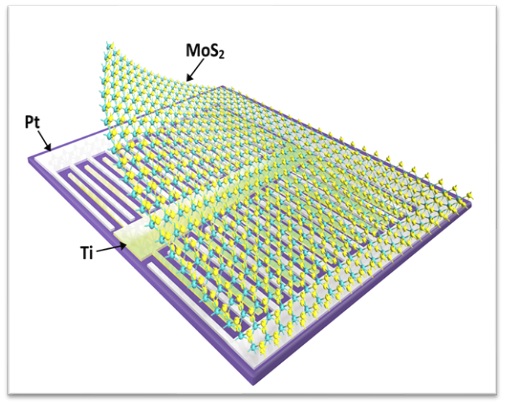
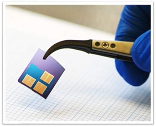
The Escarra lab particularly focuses on the synthesis of 2-dimensional semiconductors and their development into optoelectronic and photovoltaic technologies. We synthesize MoS2 and other 2-D materials using chemical vapor deposition (CVD) which is well-suited for large-area (cm-scale) growth with good thickness control in the few-layer range. Grown monolayer MoS2 and WS2 possess direct bandgaps leading to a strong light matter interaction in the visible light spectrum and more efficient light absorption per thickness than conventional semiconductors, making them leading candidates for 2-D optoelectronic and photovoltaic devices. They are particularly beneficial for space photovoltaics applications where high specific power is needed. Solar cells made using 2-D semiconductors require less material, ultimately reducing the required payload for space launch. As these materials are made, they are tested for quality using a suite of experimental techniques and ultimately developed into devices such as light emitters, detectors, and photovoltaics. Additionally, designs for space deployment of these technologies are explored and developed.
Elements of materials science, electrical engineering, chemistry and physics are combined to improve our understanding of these materials. The wealth of new information yet to be discovered makes 2-D materials an exciting frontier of science.
“The wealth of new information about these 2-D materials yet to be discovered makes this research area an exciting scientific frontier to explore.”


