
Nanophotonics and dielectric metasurfaces

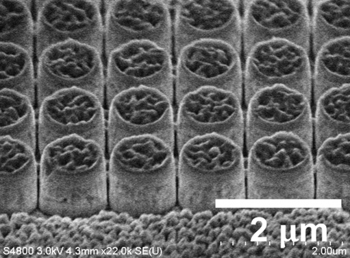
Optical metasurfaces are quasi-two-dimensional arrays of subwavelength nanoantenna elements engineered to impose abrupt, spatially dependent changes on the phase, amplitude, and polarization of incident light. Unlike conventional optics, which rely on the gradual accumulation of phase shifts as light propagates through bulk materials, metasurfaces achieve wavefront control within a layer thinner than the wavelength of light. The Escarra Group works specifically with all-dielectric and phase change Huygens metasurfaces, in which low-aspect-ratio nanoantennas support electric- and magnetic-dipole resonances. When these two resonances are tuned to spectrally overlap, it enables high-efficiency, low-loss operation across the ultraviolet, visible, and infrared regions of the spectrum. The low profile and CMOS-compatible fabrication of these devices make them practical for real-world integration.
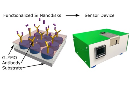
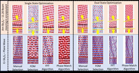
The group has demonstrated a broad range of device functionalities, spanning passive wavefront shaping, optical sensing, and active reconfigurable devices. Early work established high-efficiency gradient metasurfaces for anomalous refraction and spectrum splitting across the ultraviolet-infrared range. The strong resonant sensitivity of Huygens nanoantenna arrays to their optical environment has also been leveraged for refractive index and biosensing, culminating in a portable, low-cost sensor capable of detecting a tuberculosis biomarker at picomolar concentrations. More recently, the group’s focus has shifted toward active and reconfigurable metasurfaces. Continuously tunable independent amplitude and phase modulation has been demonstrated using vanadium dioxide Huygens metasurfaces, exploiting VO2‘s volatile insulator-to-metal transition for reversible, stable optical control at near-infrared wavelengths. In parallel, reconfigurable beam steerers and varifocal metalenses based on the nonvolatile phase-change material, antimony trisulfide, have been developed — with reversible optical switching between device states demonstrated.
The group’s current effort focuses on advancing from spatially uniform to spatially addressable dynamic metasurfaces to realize an on-chip spatial light modulator (SLM). The device under development integrates pixelated VO2 nanoantenna arrays with transparent conductive oxide microheater electrodes, enabling localized electrical control of individual pixels at near-infrared wavelengths with low drive voltages and minimal thermal crosstalk. The group aims to extend this toward two-dimensional spatial addressability, higher modulation depths, and combined amplitude and phase control within a single chip-scale device. More broadly, the volatile VO2 and nonvolatile Sb2S3 metasurface systems under development point to a new class of reconfigurable flat-optic devices with applications in optical communications, LiDAR, biomedical imaging, quantum information processing, and beyond.
“From passive wavefront shaping to electrically addressable, pixel-level control of light — the Escarra Group is developing the next generation of reconfigurable metasurfaces for chip-scale photonic applications.”