
Photovoltaics and Optoelectronics from 2D Semiconductors

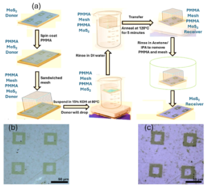
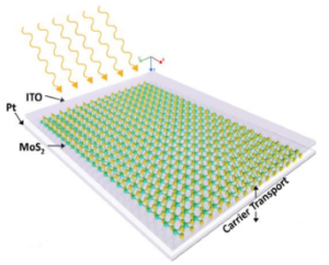

Two-dimensional (2D) transition metal dichalcogenides (TMDCs), with the general formula MX2, including materials such as MoS2, WSe2, and NbSe2, exhibit strong light–matter interactions that enable exceptionally high optical absorption and photocarrier generation despite their atomically thin dimensions. Owing to these outstanding optoelectronic characteristics, TMDCs have attracted significant attention for a wide range of applications, including transistors, sensors, memory devices, photovoltaics, flexible electronics, as well as other optoelectronic and biomedical technologies. Among these applications, TMDCs are particularly attractive for flexible, high-specific-power photovoltaic systems. For example, a monolayer of MoS2, only about 0.65 nm thick, can absorb up to 10% of incident visible light. In addition to its strong absorption capability, monolayer MoS2 possesses a direct bandgap of approximately 1.8–1.9 eV, whereas bulk MoS2 exhibits an indirect bandgap of around 1.2 eV, highlighting the significant influence of dimensionality on its electronic properties.
The Escarra Laboratory specializes in the synthesis of two-dimensional (2D) semiconductors and their integration into advanced optoelectronic and photovoltaic technologies. Materials such as MoS2 and other 2D semiconductors are synthesized using chemical vapor deposition (CVD), a technique that enables large-area (centimeter-scale) growth with precise control over thickness in the few-layer regime. Monolayer MoS2 and WS2 exhibit direct bandgaps, resulting in strong light–matter interactions within the visible spectrum and significantly higher light absorption per unit thickness compared to conventional semiconductor materials. These properties make them promising candidates for next-generation 2D optoelectronic and photovoltaic devices. In particular, they offer substantial advantages for space-based photovoltaic applications, where high specific power is critical. Because solar cells fabricated from 2D semiconductors require only minimal material, they can reduce payload mass and associated launch costs. The synthesized materials are extensively characterized using a range of experimental techniques to assess their quality and performance before being incorporated into devices such as light emitters, photodetectors, and solar cells. The laboratory also investigates and develops strategies for deploying these technologies in space environments.
“The wealth of new information about these 2-D materials yet to be discovered makes this research area an exciting scientific frontier to explore.”